- 您现在的位置:买卖IC网 > Sheet目录509 > SI4122DY-T1-GE3 (Vishay Siliconix)MOSFET N-CH 40V 27.2A 8-SOIC
�� �
�
�VISHAY� SILICONIX�
�TrenchFET� ?� Power� MOSFETs�
�Application� Note� 808�
�Mounting� LITTLE� FOOT� ?� ,� SO-8� Power� MOSFETs�
�Wharton� McDaniel�
�0.2� 88�
�Surface-mounted� LITTLE� FOOT� power� MOSFETs� use�
�integrated� circuit� and� small-signal� packages� which� have�
�7.3�
�been� been� modified� to� provide� the� heat� transfer� capabilities�
�required� by� power� devices.� Leadframe� materials� and�
�design,� molding� compounds,� and� die� attach� materials� have�
�been� changed,� while� the� footprint� of� the� packages� remains�
�the� same.�
�See� Application� Note� 826,� Recommended� Minimum� Pad�
�Patterns� With� Outline� Drawing� Access� for� Vishay� Siliconix�
�0.050�
�1.27�
�0.027�
�0.69�
�0.07� 8�
�1.9� 8�
�0.2�
�5.07�
�0.0� 88�
�2.25�
�0.0� 88�
�2.25�
�MOSFETs,� (� http://www.vishay.com/ppg?72286� ),� for� the�
�basis� of� the� pad� design� for� a� LITTLE� FOOT� SO-8� power�
�MOSFET.� In� converting� this� recommended� minimum� pad�
�to� the� pad� set� for� a� power� MOSFET,� designers� must� make�
�two� connections:� an� electrical� connection� and� a� thermal�
�connection,� to� draw� heat� away� from� the� package.�
�In� the� case� of� the� SO-8� package,� the� thermal� connections�
�are� very� simple.� Pins� 5,� 6,� 7,� and� 8� are� the� drain� of� the�
�MOSFET� for� a� single� MOSFET� package� and� are� connected�
�together.� In� a� dual� package,� pins� 5� and� 6� are� one� drain,� and�
�pins� 7� and� 8� are� the� other� drain.� For� a� small-signal� device� or�
�integrated� circuit,� typical� connections� would� be� made� with�
�traces� that� are� 0.020� inches� wide.� Since� the� drain� pins� serve�
�the� additional� function� of� providing� the� thermal� connection�
�to� the� package,� this� level� of� connection� is� inadequate.� The�
�total� cross� section� of� the� copper� may� be� adequate� to� carry�
�the� current� required� for� the� application,� but� it� presents� a�
�large� thermal� impedance.� Also,� heat� spreads� in� a� circular�
�fashion� from� the� heat� source.� In� this� case� the� drain� pins� are�
�the� heat� sources� when� looking� at� heat� spread� on� the� PC�
�board.�
�0.2� 88�
�7.3�
�0.050�
�1.27�
�0.196�
�5.0�
�0.027�
�0.69�
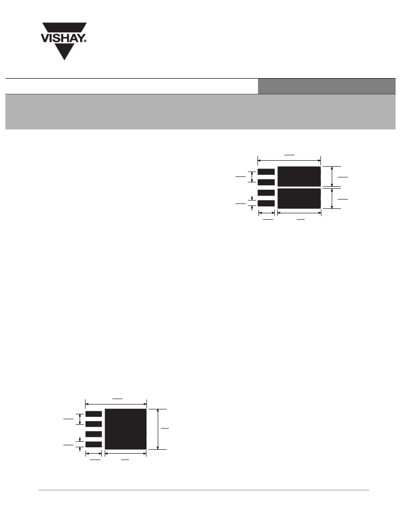
�Figure� 2.� Dual� MOSFET� SO-8� Pad� Pattern�
�With� Copper� Spreading�
�The� minimum� recommended� pad� patterns� for� the�
�single-MOSFET� SO-8� with� copper� spreading� (Figure� 1)� and�
�dual-MOSFET� SO-8� with� copper� spreading� (Figure� 2)� show�
�the� starting� point� for� utilizing� the� board� area� available� for� the�
�heat-spreading� copper.� To� create� this� pattern,� a� plane� of�
�copper� overlies� the� drain� pins.� The� copper� plane� connects�
�the� drain� pins� electrically,� but� more� importantly� provides�
�planar� copper� to� draw� heat� from� the� drain� leads� and� start� the�
�process� of� spreading� the� heat� so� it� can� be� dissipated� into� the�
�ambient� air.� These� patterns� use� all� the� available� area�
�underneath� the� body� for� this� purpose.�
�Since� surface-mounted� packages� are� small,� and� reflow�
�soldering� is� the� most� common� way� in� which� these� are�
�affixed� to� the� PC� board,� “thermal”� connections� from� the�
�planar� copper� to� the� pads� have� not� been� used.� Even� if�
�additional� planar� copper� area� is� used,� there� should� be� no�
�problems� in� the� soldering� process.� The� actual� solder�
�connections� are� defined� by� the� solder� mask� openings.� By�
�combining� the� basic� footprint� with� the� copper� plane� on� the�
�drain� pins,� the� solder� mask� generation� occurs� automatically.�
�A� final� item� to� keep� in� mind� is� the� width� of� the� power� traces.�
�The� absolute� minimum� power� trace� width� must� be�
�determined� by� the� amount� of� current� it� has� to� carry.� For�
�0.07� 8�
�1.9� 8�
�0.2�
�5.07�
�thermal� reasons,� this� minimum� width� should� be� at� least�
�0.020� inches.� The� use� of� wide� traces� connected� to� the� drain�
�Figure� 1.� Single� MOSFET� SO-8� Pad�
�Pattern� With� Copper� Spreading�
�Document� Number:� 70740�
�Revision:� 18-Jun-07�
�plane� provides� a� low� impedance� path� for� heat� to� move� away�
�from� the� device.�
�www.vishay.com�
�1�
�发布紧急采购,3分钟左右您将得到回复。
相关PDF资料
SI4126DY-T1-GE3
MOSFET N-CH 30V 39A 8-SOIC
SI4134DY-T1-E3
MOSFET N-CH D-S 30V 8-SOIC
SI4158DY-T1-GE3
MOSFET N-CH D-S 20V 8-SOIC
SI4170DY-T1-GE3
MOSFET N-CH 30V 30A 8-SOIC
SI4174DY-T1-GE3
MOSFET N-CH D-S 30V 8-SOIC
SI4186DY-T1-GE3
MOSFET N-CH 20V 35.8A 8SOIC
SI4190ADY-T1-GE3
MOSF N CH 100V 18.4A SO8
SI4214DDY-T1-E3
MOSFET 2N-CH 30V 8.5A SO8
相关代理商/技术参数
SI4122-EVB
功能描述:射频开发工具 Single-Band RF Synth (RF2/IF) Eval TSSOP RoHS:否 制造商:Taiyo Yuden 产品:Wireless Modules 类型:Wireless Audio 工具用于评估:WYSAAVDX7 频率: 工作电源电压:3.4 V to 5.5 V
SI4122G
制造商:SILABS 制造商全称:SILABS 功能描述:DUAL-BAND RF SYNTHESIZER WITH INTEGRATED VCOS FOR GSM AND GPRS WIRELESS COMMUNICATIONS
SI4122G-BM
制造商:未知厂家 制造商全称:未知厂家 功能描述:DUAL-BAND RF SYNTHESIZER WITH INTEGRATED VCOS FOR GSM AND GPRS WIRELESS COMMUNICATIONS
SI4122G-BMR
功能描述:锁相环 - PLL CONTACT SILICON LABS FOR AVAILABILITY RoHS:否 制造商:Silicon Labs 类型:PLL Clock Multiplier 电路数量:1 最大输入频率:710 MHz 最小输入频率:0.002 MHz 输出频率范围:0.002 MHz to 808 MHz 电源电压-最大:3.63 V 电源电压-最小:1.71 V 最大工作温度:+ 85 C 最小工作温度:- 40 C 封装 / 箱体:QFN-36 封装:Tray
SI4122G-BT
制造商:SILABS 制造商全称:SILABS 功能描述:DUAL-BAND RF SYNTHESIZER WITH INTEGRATED VCOS FOR GSM AND GPRS WIRELESS COMMUNICATIONS
SI4122GM-EVB
制造商:Silicon Laboratories Inc 功能描述:
SI4122M-EVB
功能描述:射频开发工具 Single-Band GSM RoHS:否 制造商:Taiyo Yuden 产品:Wireless Modules 类型:Wireless Audio 工具用于评估:WYSAAVDX7 频率: 工作电源电压:3.4 V to 5.5 V